
Following on from our articles on the Unbalanced piezo preamp and Guitar leads, buffers and true bypass we present a project to build your own JFET buffer pedal. The circuit is essentially the same as in the unbalanced piezo preamp with a few tweaks and may be built into a Hammond 1590B or similar stomp-box enclosure. Here’s the schematic:
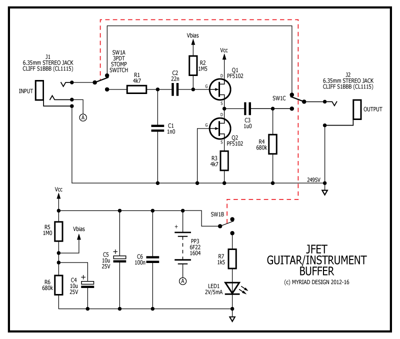
This is an impedance buffer rather than a preamp as it has no voltage gain (in fact the voltage gain is slightly less than unity). Battery life is a few hundred hours and the design will work down to about 4V. The design has very low noise and distortion.

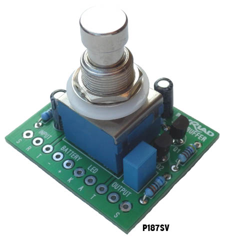
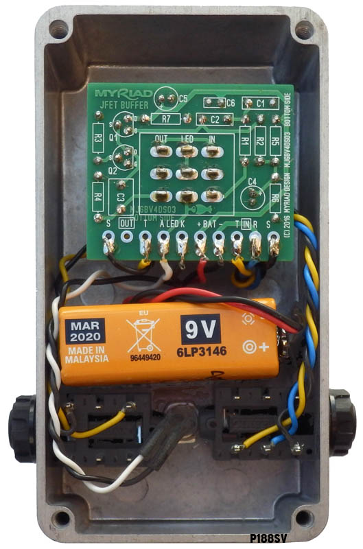
Dimensions are 43mm x 37mm and the PCB is designed to solder directly to an industry-standard 3PDT mechanical stomp switch. Connections are for input jack, output jack, LED and battery. Insertion of the input jack switches power on.
If you want to experiment with the design, here’s the low down:
- R1 and C1 form a low-pass filter to keep RF interference out of the system.
- C2 sets the low-frequency response at the input.
- R2 sets the input impedance. You can increase this up to about 10M Ohms.
- R3 sets the bias current in Q1.
- C3 sets the low-frequency response at the output.
- R4 applies a nominal load to the output to discharge C3 and avoid thumps.
- R5, R6 set the d.c. operating point at the source of Q1 (which should be about 1/2 Vcc).
- R7 sets the LED brightness and will need to be adjusted to suit.
Playing with component values…
For those of you who want to play with component values or who do not have the exact values as above, here’s the low-down:
R1 and C1 form a low-pass filter which keeps RF signals out of the preamp. With the values above, the -3dB point is about 33kHz. If you decrease C1 you will raise the upper 3dB point. C1=470pF will increase the -3dB point to about 72kHz. If you increase R1 to 10k, the -3dB point falls to about 19kHz. You can leave out C1 altogether if you wish, but the upper -3dB point rises to about 6MHz.
C2 sets the low-frequency response at the input of the buffer. Any value between 10n and 100n will be OK.
R2 sets the input impedance. Anything between about 470k and 20M is good. However, resistors over a few MOhm (particularly carbon film resistors) can be quite noisy.
Q2 and R3 form a constant (bias) current sink for Q1. The value of the bias current is not critical and to maximise battery life should be between about 70 and 200uA (i.e. 0.07 to 0.2mA). A value of 4k7 with a PF5102 of Idss about 6mA will give a current of about 140uA. You can use pretty much any general purpose JFETs for Q1 and Q2, such as 2N5457/8/9, 2N5484/5/6, PF5102/3 all of which have the same pinout. You can also use BF256B, but they have a different pinout. Start with 4k7 for R3 and measure the d.c. voltage across R3 with no signal applied. Bias current is measure voltage divided by the value of R3. Increase R3 to decrease bias current and vice versa.
C3 sets the low-frequency response at the output of the circuit. It needs to be much bigger than C2 because the input impedance of the next stage may well be as low as 10k, which gives a -3dB point at about 16Hz. However, most guitar amps have an input impedance above about 33k (worst case), so you could reduce C3 to 470nF or even 220nF if you don’t have a 1uF film capacitor to hand. Otherwise, you could use a 10uF 16V electrolytic with positive towards Q1 and Q2.
R4 could be anything between 100k and 1M Ohms. The lower the value, the better at reducing switching noise, but lower the value the more the low-frequency response is reduced. The value of 680k shown above is just to make it the same as R6.
R5 and R6 set the d.c. operating point at the drain-source junction. Note that in a lot of circuits R5 and R6 would be the same value, but here we are biasing the circuit at the gate of Q1 in order to get 1/2Vcc at the source of Q1 to give maximum voltage swing at the output. If you don’t have these values to hand, don’t worry, you can use two resistors the same value anywhere from about 33k to 1Meg. However, the lower the value of R5, R6 the more current they draw from the battery, so the higher the better. Connect your meter to ground and check that the d.c. voltage at the source of Q1 is about 1/2Vcc or thereabouts with no signal present.
R7 sets the current for the LED and should be adjusted to suit. Don’t forget that the LED is by far the biggest load on the battery, so the lower the LED current the longer the battery will last.
If you are using a 9V battery only, you can safely omit C5 and C6. C4 and C5 could be anything between 4u7 and 47uF and C6 could be 10n instead of 100n.
Have fun. ![]()
Hi, is there any reason you didn’t use the LED to produce the bias voltage? Most blue LEDs have a vf of about 3.3 volts similar to the Vbias potential divider.
With the 680k and 1M resistors, the bias voltage is set at about 3.6V with a nominal 9V supply. This gives a bias point of 4.5V at the input side of C3 to give maximum voltage swing at the output. You could use a white or blue LED to generate bias voltage; however, there are several reasons why this would not be optimal. Firstly, bias voltage would be fixed instead of varying with the battery voltage. Secondly, an LED is more expensive than resistors. Thirdly, the bias current would have to be much higher than the few microamps consumed by the resistor divider (which would drain your battery faster than necessary) and lastly, stomp pedals of this type do not routinely have an LED to show they are powered up (although there’s no reason why they couldn’t/shouldn’t). HTH.