I’ve had some interest in and feedback for my Altoids Piezo DI box and I have revised the design sufficiently to warrant a new post. The new design has the following changes from the previous version:
- 1/4″ jacks on input and output
- Low-voltage monitor (TC54) on the battery supply
- Higher voltage zener (33V)
- Increase R7 & R8 to 1M0 (or eliminate them entirely)
- Asymmetric bias voltage
- Unity gain op-amp circuit
- Reduce C4 from 470nF to 100nF
These changes have been made to reduce power consumption, free-up space on the PCB and reduce cost.
Here’s the revised schematic:
And here’s a photo of the prototype PCB:
I had to ditch the switch-with-integrated-LED because it took up too much real estate on the PCB. Also, I have specified Cliff S1 style jack sockets because they take up less space on the PCB and are lower-profile than standard sockets. The Altoids lid fits better with the lower-profile sockets.
If you can get Cliff sockets with a “special nose” (half threaded) all the better. You can buy them from the Stompville shop here.
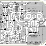
Here’s the PCB layouts (the foil is at 600 dpi):
As with the previous design, the input socket is the lower of the two. R16 and R17 set up the TC54 to turn the LED on when the battery voltage falls to about 7.3V. When phantom powered (from 48V), the voltage between pin 8 and pin 4 of the op-amp should be a little less than 30V. All 1/8W resistors except for R13.
Note that Q1 and the op-amp require different bias voltages. This is because the source resistor in Q2 raises the operating point of Q1. R14 and R15 have been selected as a compromise to reduce component count. You should find that the d.c. voltage at the source of Q1 is a little higher than 1/2Vcc and the voltage at pin 5 of the op-amp (both measured with respect to ground) is a little lower than 1/2Vcc. ![]()


