
I thought I would make myself a crib sheet for the basics of designing with op amps. Then I thought I may as well post it here so I won’t have to remember where I put my crib sheet. This will be an ongoing thing.
The subject is: Analogue audio design using op-amps with single-ended supply.
Reference reading material
- Op Amps For Everyone by Ron Mancini – Texas Instruments, 2002
- Handbook Of Operational Amplifier Applications by B. Carter and T. R. Brown – Burr Brown, 2001
- Demystifying Single-Supply Op-Amp Design by C Kitchen – Analog Devices, 2002
- Single-Supply Op-Amp Design Techniques SLOA030A by Texas Instruments, 2002
- Single-Supply Op-Amp Circuit Collection SLOA058 by Texas Instruments, 2000
- Using Single Supply Operational Amplifiers in Embedded Systems By B Baker – Microchip AN682, 2000
Please report any broken links by email. Thanks.
Ideal op-amp characteristics
- Voltage gain (Av) infinitely high
- Differential input voltage (Ve) = zero
- Input current (Ib) = zero
- Input impedance (Zin) infinitely high
- Output impedance (Zout) = zero
Ideal Inverting Amplifier
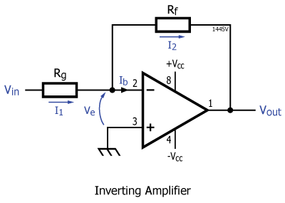
- Note that the ideal amp has split (dual) supply +Vcc and -Vcc
- Non-inverting input (+) is grounded. Assume Ve = zero, so inverting input (-) is also grounded
- Assume Ib = zero, so no current flows into the op-amp and I1 must equal I2
- Therefore I1 = Vin / Rg and I2 = Vout / Rf giving
- Vout/Vin = Rf/Rg but this is an inverting amplifier so Vout = -Vin. (Rf/Rg)
Ideal Non-Inverting Amplifier

- Note that the ideal amp has split (dual) supply +Vcc and -Vcc
- Assume Ve = zero, so Vin appears at inverting input (-) giving Vrg = Vin
- Therefore Vin = Vout .Rg/(Rf+Rg) or Vout = Vin. (1+ Rf/Rg)
Single-supply overview
An audio signal is an a.c. signal usually with no d.c. offset which varies either side of ground (zero volts). If the audio signal has a d.c. offset we can remove it with a coupling capacitor. The problem with having a only a single rail supply (i.e. +Vcc and ground) is that when the input goes negative with respect to ground, there’s nowhere for the output to go.
The way we get around this problem is to create a virtual ground at 1/2 Vcc using a potential divider. Effectively we introduce a d.c. offset to the incoming audio signal so that instead of varying between +/- 500mV peak (say) it now varies between +4V and +5V centered around a virtual ground of +4.5V. If our amplifier has an a.c. gain of 2, the output will vary between +3.5V and +5.5V. Clearly we don’t want the amplifier to have a d.c. gain or the amplifier will try to turn our +4V to +5V signal into a +8V to +10V signal and (as our power supply is only 9V) this will not work.
There are a few ways of creating our virtual ground point (sometimes called Vbias or Vb) but the most common way is to to use a simple voltage divider.

Current Ib flows through the potential divder all the time the battery is connected and may contribute significantly to battery drain. For example, in Boss pedals, the combined value of R1 and R2 is often 20k, leading to a current Ib of approximately half a milliamp. Higher values for R1 and R2 minimise current drain, but make the supply less ‘stiff’.
Sometimes (e.g. with a JFET input stage) the active device alters the operating point. In this case we can adjust the bias voltage applied to the input of the stage so that the signal at the output of the stage is centered at 1/2Vcc. Also, some op amps are able to drive the output closer to (say) ground than the positive rail, so the operating point (i.e. bias voltage) again may have to be altered to give the maximum swing in both directions at the output.
- Low values for R1 and R2 improve stiffness
- Low values for R1 and R2 improve low-frequency performance
- Low values for R1 and R2 improve PSRR (power supply rejection ratio)
- High values for R1 and R2 reduce quiescent current consumption
- High values for R1 and R2 are more prone to noise (high = in excess of 1M Ohm)
- Higher values for C1 and C2 (typically 100u and 47u respectively) improve stiffness and PSRR
Two alternatives to the simple voltage divider are the buffered voltage divider and proprietary rail-splitter integrated circuits such as the TLE2426.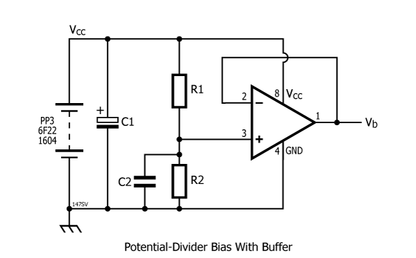
- R1 and R2 can be increased compared to simple voltage divider
- C2 can be reduced compared to simple voltage divider
- Output impedance is reduced to ~ 10 Ohms (often less, depending on the op amp used)
- Quiescent current increased if op-amp isn’t low power
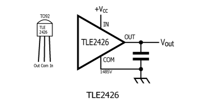
- Very stiff – output impedance rises to 1Ohm @ 10kHz
- Can sink/source 20mA
- Low quiescent current ~ 0.25mA @ 9V Vin
- Small footprint
- Output capacitor 1uF minimum for stable operation (see data sheet Fig 17)
Checklist for choosing an op-amp
- Supply voltage – is it suitable for your supply? – will it still work when your battery is failing?
- Supply current – is it going to drain your battery too quickly?
- Output voltage swing – will it go rail to rail (useful with a failing battery)?
- Output current sink/source – Is it man enough? Probably not an issue, but may be a consideration.
- Slew rate – at least 2V/us (for audio).
- Gain-bandwidth product – generally not a problem unless you’re designing microphone preamps.
- Input impedance – FET input op amps have super high input impedance, bipolar input much less so.
- Input offset voltage – gets amplified!
- Unity-gain stability – don’t attenuate or make a voltage follower/buffer if not stable at unity-gain.
- CMRR (common mode rejection ratio) – the higher the better!
- Noise – the lower the better!
Standard single-supply circuits
Non-inverting unity gain buffer

- R isolates this stage from the Vbias rail, reducing noise and interaction (improves PSRR)
- C isolates the previous stage from the bias voltage supplied via R
- R effectively sets the a.c. input impedance of the stage
- RC form a high-pass (low-cut) filter which affects the frequency response of the stage
Non-inverting amplifier
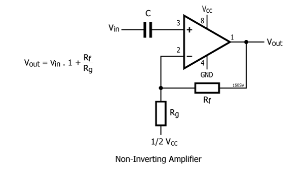
- A.C. input impedance = Rf || Rg
- C and Rf||Rg form a high-pass (low-cut) filter which affects the frequency response of the stage
- Value of C is not important unless Rf and Rg are very low (e.g. 100~1000 Ohms)
Non-inverting amplifier – alternative
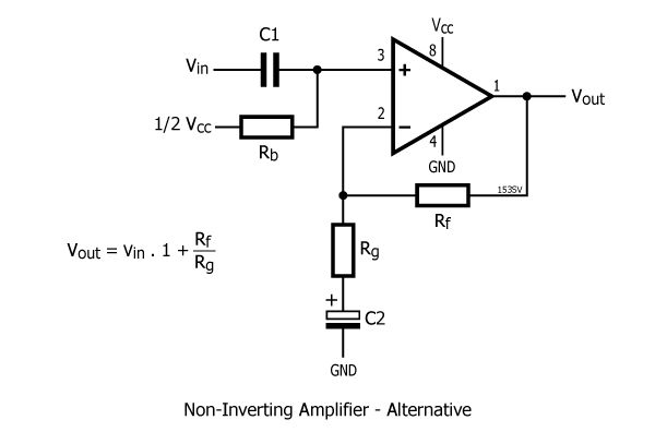
- If C2 is too low, there will be a high-pass (low-cut) filter effect fc = 1/(2Pi.Rg.C2)
- Rb sets a.c. input impedance
- C1 and Rb form a high-pass (low-cut) filter which affects the frequency response of the stage
- Note that C2 references to GND not Vcc/2
Non-inverting attenuator

- This is simply a passive potential divider with a unity gain buffer
- C and (R1 + R2) form a high-pass (low-cut) filter which affects the frequency response of the stage
- R1 + R2 is the a.c. input impedance
- Use a similar arrangement for inverting attenuator (i.e. potential divider followed by inverting buffer)
Inverting amplifier

- Rg sets the a.c. input impedance
- Rb = Rf || Rg for minimum error due to input bias current
- C and Rg form a high-pass (low-cut) filter which affects the frequency response of the stage
Rolling off the high-frequency response
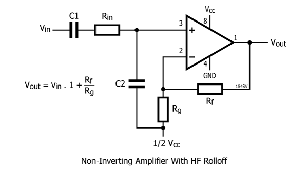
- Rin, C2 form low pass filter Fc = 1/(2.Pi.Rin.C2)

- Does not require extra resistor compared with non-inverting topology
- Rf, C2 form low pass filter Fc = 1/(2.Pi.Rf.C2)
Op amp protection
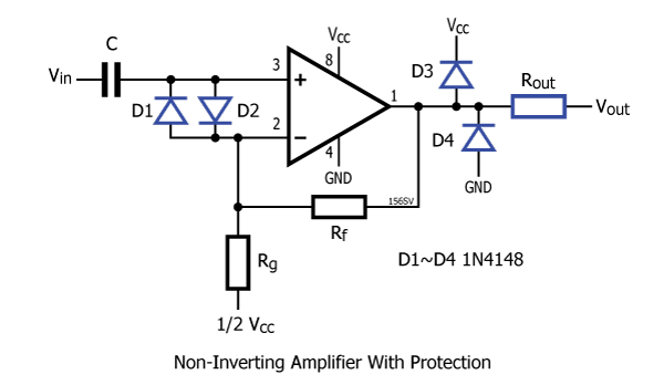
Ideally Ve – the differential input voltage (i.e. the voltage between pins 2 and 3) – is zero (as a result of the open loop gain ideally being infinity).
Resistors Rf and Rg feed back a proportion of the output voltage to the inverting input. The op amp will continuously adjust its output voltage so that the voltage at the inverting input is the same as the non-inverting input. The voltages at the non-inverting and inverting inputs will then sum to zero.
D1 and D2 clamp the differential voltage to +/- 0.6V (i.e. the Vf of a 1N4148) thus providing some protection to the input. Note that this does not mean that the input signal is limited to +/- 0.6V before clipping as the input signal is referenced to ground.
Rout, D3 and D4 protect the output stage of the op amp. If the output gets driven (by some external voltage source) more than 0.6V higher than the positive rail then D3 will conduct and clamp the voltage at the output of the op amp to Vcc + 0.6V. Similarly, D4 will clamp the op amp output at a minimum of -0.6V. Rout serves to limit the current flowing in the protection diodes. A suitable value for Rout is 33 Ohms. Note that this will set the output impedance of the stage at 33 Ohms and may affect the frequency response of the following stage. ![]()
Hello, really good stuff to show the diagram titled “Non-inverting amplifier – alternative”. Meanwhile, I just can not derive the output voltage Vout with respect to GND as a function of the input voltage Vin wrt GND. Does anybody know how to do it ?
Thank you in advance, Théo
The gain equation as shown above is simplified. For further information see Mancini, Op Amps For Everyone, Section A.3.19