Update: Kits available in the shop here.
I finally got round to revisiting the manual JFET matcher project. Please take a look at the earlier article and refresh yourself on the details of the three tests we can perform to help match JFETs:
- Vgs(off) – which we approach with a gate-source resistance of 10M Ohms
- Vgs(10k) – the gate-source voltage when the drain-source resistance is 10k
- Idss – the current which flows in the drain-source channel when Vgs = zero

The circuit board stands on insulating pillars and is designed to be used on the workbench as-is (i.e. without an enclosure). The tester may be powered from a 9V battery or an external power pack. The unit accepts a power supply with a 2.1mm d.c. power plug (tip/centre negative) with a voltage between 9 and 18V d.c. A standard (Electro-Harmonix/Boss/Pearl/Ibanez) effects pedal PSU will be suitable.
There are 4mm banana sockets for the connection of two meters – one to measure current and one to measure voltage. You can measure Idss without a voltmeter present but you can’t measure Vgs without either having an ammeter in place or shorting out the ammeter terminals. There is a switch to select whether or not there is an ammeter in-circuit.
Other controls include a power switch; a polarity switch to select between n-channel or p-channel JFETs; a selector switch to select between Vgs(M), Vgs(k) and Idss; a jumper to select between two resistance values for Vgs(k) (see Note 1, below); and a push switch to enable the Idss current. A zero-insertion-force (ZIF) socket accepts the JFET under test.

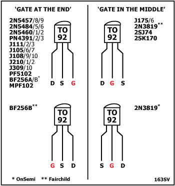
It turns out that common TO92 JFETs generally have one of two pinouts (DSG or DGS). Sometimes the pinout is GSD or SGD – but this means the device can simply be inserted in the socket back-to-front. See also Note 2, below.
The Idss current has a heating effect on the drain-source channel of the JFET – increasing its resistance and thus reducing Idss. It is almost impossible to manually get a value for Idss at 20-30mA because the current drops faster than the average multimeter updates its display. At lower Idss values the reading is stable over a few seconds. Either way, the ‘TEST Idss’ button must be pressed to pass a current through the JFET.
Note that the schematic shows either TL071 or OPA244 for the op-amp. The TL071 could be any general purpose op-amp (e.g. half of an RC4558, TL072, LM833, etc). The OPA244 has the advantage of rail-to-rail output voltage swing. This means that you can characterise a wider range of JFETs with only battery power or a 9V supply. The OPA244 is the cheapest suitable rail-to-rail op-amp I could find in Farnell. If anyone has any other suggestions please leave a comment below. If you raise the supply voltage then the need for a rail-to-rail op-amp is reduced.
Finally, it is worth noting that when matching JFETs, we are not trying to measure absolute values for Vgs(M), Vgs(k) and Idss. We are merely trying to find pairs or sets of JFETs that give similar (and preferably identical) results to each other when measured at the same time under the same test conditions.
Kits are available in the shop here.

Note 1. In the previous article, we use RG Keen’s circuit to find the value of Vgs when the drain-source resistance is 10k. This is important for some phaser designs. Whilst designing the pcb for the new matcher, I decided to allow for two different resistance values, selected by a jumper. The second resistor could be anywhere between (say) 1k and 1M to suit a particular design. I currently have no idea whether this feature will be of any utility to anyone. On my prototype, I arbitrarily chose 4k7 for the alternative resistor.
Note 2. Sometimes different manufacturers will show S and D swapped for the same part number but usually this occurs when S and D are interchangeable (i.e. the internal structure of the JFET is symmetrical and labelling the ends of the drain-source channel is arbitrary).
![]()

